Creating SoCat-57 Part 1
In this first article I will tell you how I came to create a new printed circuit board for some old hardware, specifically a Socket 5-to-7 CPU power interposer and what that looks like.
The Background
About late in September 2021 I began more actively working with my apparently extremely rare Sprint P5N-DP-v3 motherboard. This is a dual Socket 5 motherboard created by then one of the founding/parent companies created by the now CEO of Foxconn. More on that crazy history in a future article.
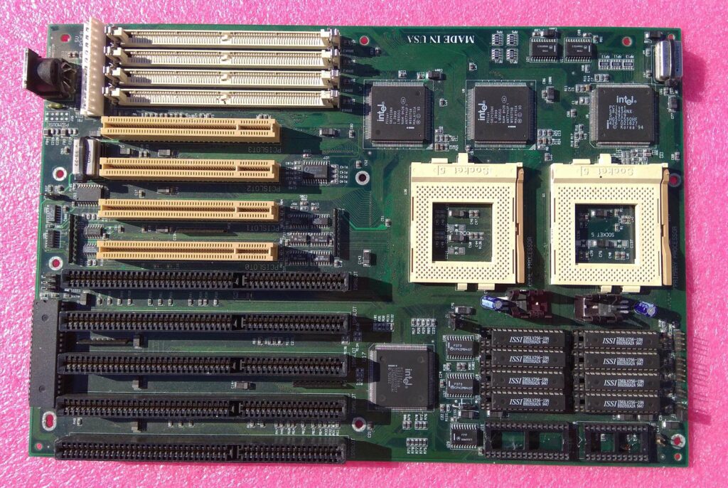
Sprint Manufacturing P5N-DP-V3 before repair work started. I removed the BIOS and RTC chip for recovery and modificaiton.
Also a big thanks to the folks over at UltimateRetro.net for even making it possible for me to identify this motherboard. Without you this would have been a bit more difficult.
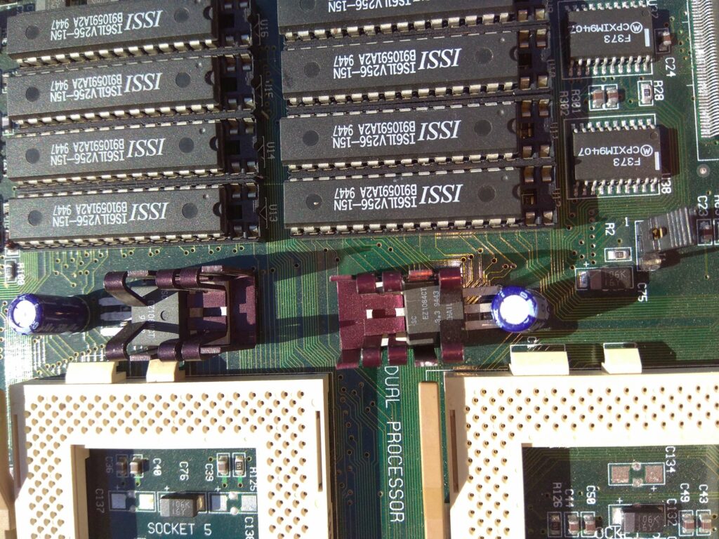
The Sprint P5N or P5N as I will call it from now on is one of those very early 430NX based dual socket 5 Pentium 60/75/66 and 90/120 Mhz only motherboards. It runs solely from AT power, has 4 slots of 72 pin SIMM memory slots and most importantly powers the CPU’s single IO and Core voltage each from an Semtech branded EZ1084CT-3.3T Fixed (3.3V) linear regulators rated at 5A each. Why does this matter? Well chiefly this means that my mainboard is limited to only supporting 3.3V single voltage processors. Newer more interesting processors use a split voltage supply configuration which requires 3.3V for the IO signals and anywhere from 2.1 to 3.5V for the Core itself.
The EZ1084 is one of the many LT1084 variants and is semi-passively cooled from the CPU heatsinks airflow with some purple ThermAlloy heatsinks. These as I found do an absolute horrible job of cooling the regulators. Since they are not even attached to the motherboard or any other larger thermal mass.
These linear regulators also have the downside of being soldered into the board via a single tiny poorly placed through hole pin that carries all of the processor current. But to complicate matters the second regulator on the second processor powers not only the CPU but also the Asynchronous SRAM cache on the motherboard. All 8 chips of it.
Initially while repairing this motherboard (it was DOA) I found that not only where the original regulators degraded, likely by long hours of operation with limited airflow, but also the voltage output from them would cause intermittent issues with the cache composed of 8x 3.3V ISSI 61LV256-15N chips (total 256KB) .Ontop of that the BIOS was also corrupted beyond repair, but that is another story of how I adapted Award 4.51 to run on a formerly AMIBIOS 10/10/94 machine.
PS: If you happen to have the BIOS for the sprint P5N-DP or even just a board/chip please get in touch.
Failed EZ1084 on the right. Also pictured are the horrible Thermalloy heatsinks.
They are simply crimped in place without any thermal interface material.
Then one day while testing in single processor configuration, the secondary regulator failed entirely and ended up sending 5V into the cache array.
This lead me to replace them in their entirety along with installing new LT1084 7.5A rated regulators. Miraculously the SRAM chips still somehow tested good in my chip tester, but would not function correctly on the board. I suspect some of the ouput drivers became degraded out of spec for the board but were still good to drive the more sensitive tester.
Over time the board was also modified to enable the use of the full multiplier range and did indeed become capable of running 200Mhz Pentiums safely at length with some air cooling over the Regulators. But ultimately I wanted to run more. 233/266 MHz pentiums and overclocking the frontside bus to 75Mhz or so was what I wanted to really test.
A Solution
After much probing of the motherboard I concluded it was not safe to modify the board to split the power planes, besides as far as I knew this board was a one of a kind board. At least I haven’t seen any others… Yet.
Thus began the search for some old Socket 5-to-7 interposer devices such as the Kingston TurboChip or Evergreen PowerLeap.
One look at ebay left me wincing in pain as If my wallet just stopped a bullet.
They were either not available at all or the few I could find were selling for hundreds of dollars. My budget was about $30 at most. And I had just missed a broken one that sold for $25.25.
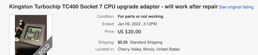
TurboChip listing I missed.
And I wanted, no, I needed two. What fun is a dual socket board if you can only use one processor?
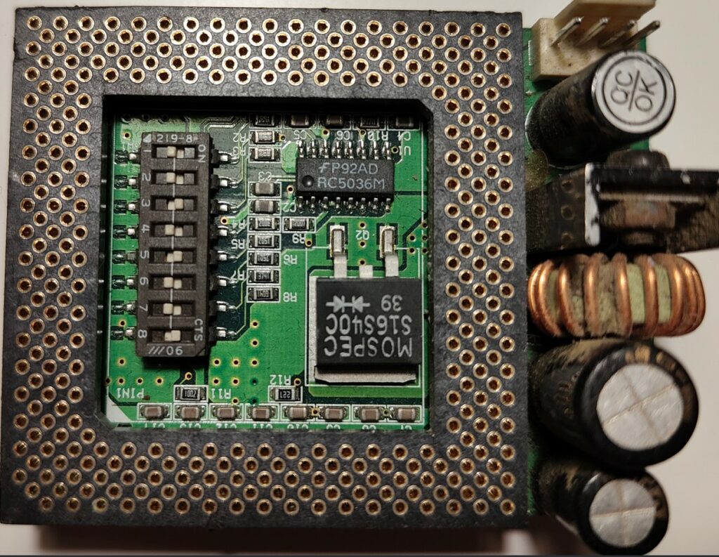
But this listing did provide some insight into how Kingston engineers had built this adapter. Evidently nothing more than a RC5057M synchronous regulator driving your average two N-channel MOSFETs with a small assortment of passives.
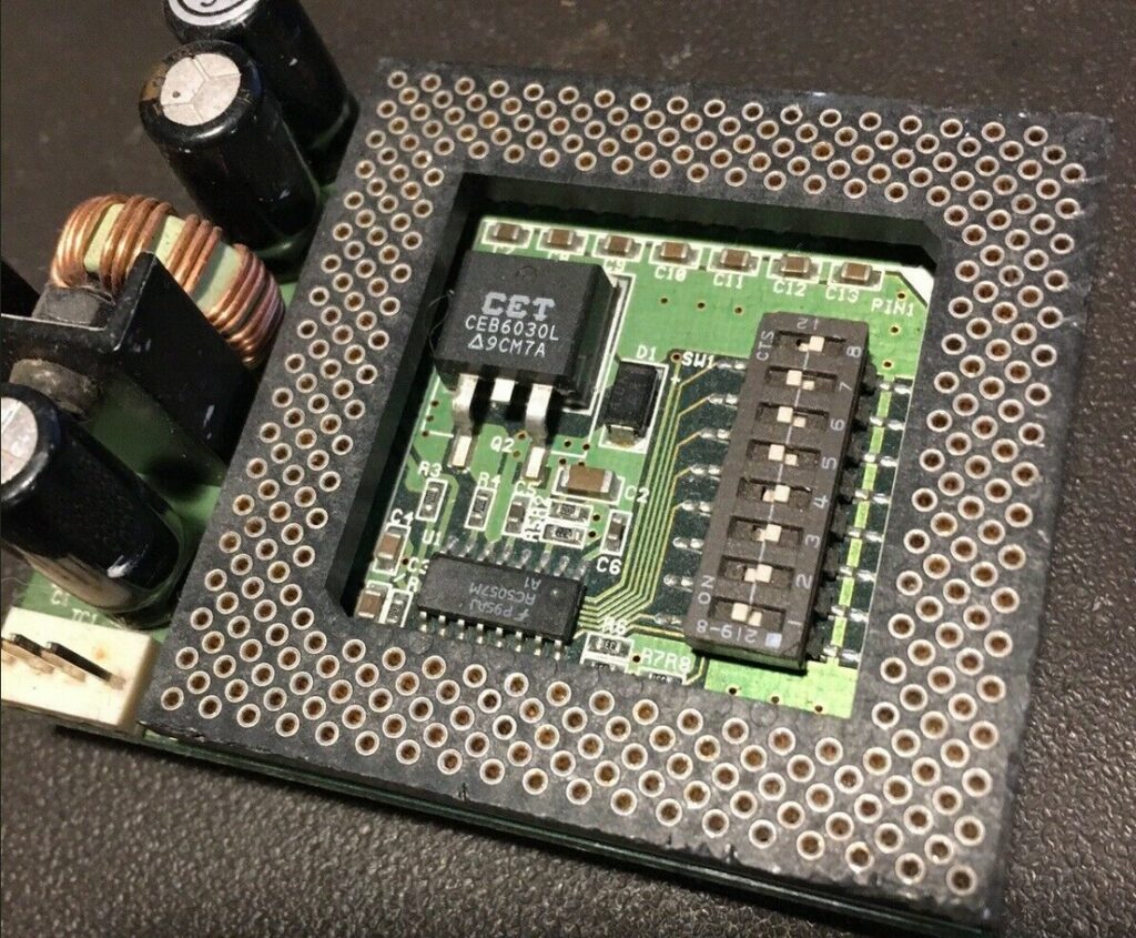
TurboChip TC400 variant that uses a dual N-Channel Mosfet regulator arrangement
The circuit for this is approximately identical to the one given in the reference documentation of the RC5057M. However as you might spot now already we are dealing with a (by modern standards) rather odd 12V + 5V control arrangement. The 12V is used to power the RC5057M’s gate drivers and the 5V itself is used for the MOSFET High-side input. A somewhat undesirable combination for a modern version if we want to drive it entirely from the now ubiquitous 12V sources.
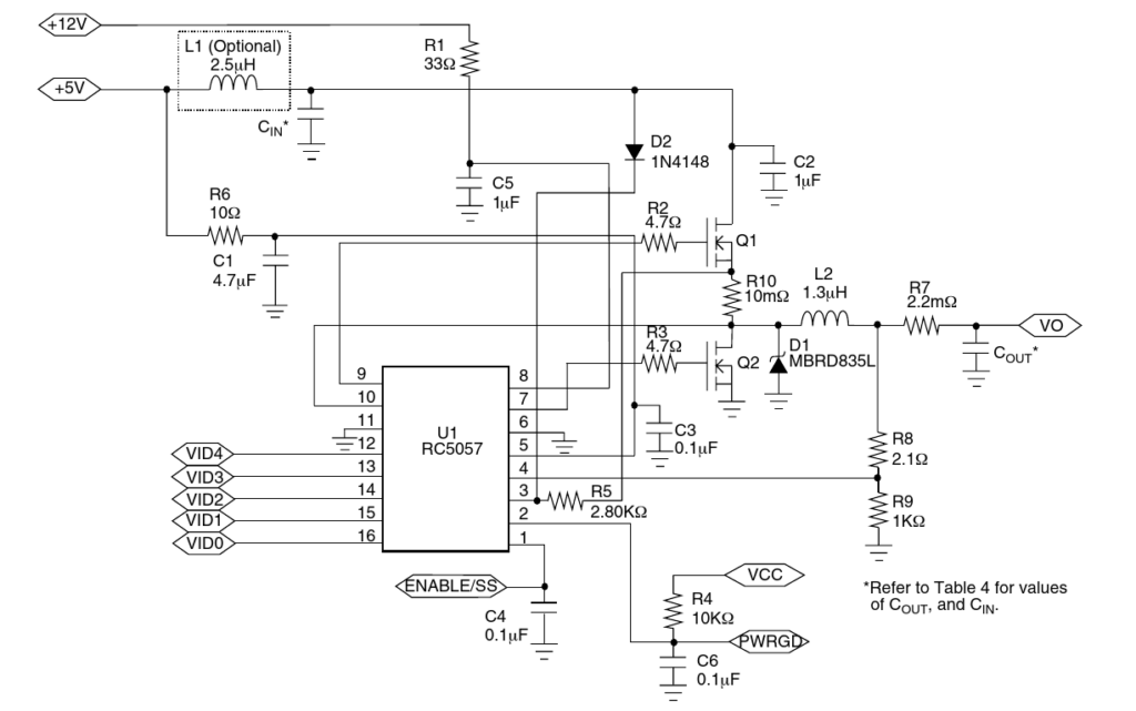
Earlier versions of this Adapter also used the Raytheon RC5036M regulator itself a resistance programmed device. By switching together various combinations of resistors a range of desirable voltages could be achieved. This can be seen in the picture sent to me by my friend Carlos.
Earlier Tubochip variant that uses the RC5036 with a Mosfet+ Diode regulator arrangement. Picture Credit: Carlos S.M.
This is effectively the same but less efficient regulator arrangement than found on the TC400.
More interesting however were the rest of pictures Carlos sent me, specifically how the sockets where assembled. I had a hunch that it was nothing more than two sockets stacked on-top of each other through the PCB, with the VCC2 (Vcore pins) removed.
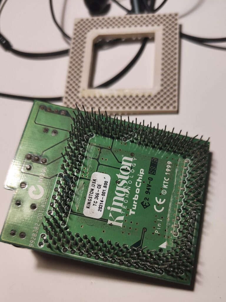
Disassembled Earlier TuboChip variant showing pin arrangement. Picture Credit: Carlos S.M.
As can be seen in the above image this hunch proved to be correct. Carlos had successfully managed to pry the bottom plastic frame off his TurboChip. (The pins were already damaged before). But more importantly from a side view it became obvious that Kingston had stacked and then soldered together two sockets. The soldering aspect turns out to be important later.
Furthermore it becomes obvious which pins have been cut off from the socket. We can clearly see that a number of Core voltage VCC2 around the outer edges and Multiplier BF[0:2] pins have been cut on the underside of the PCB and are marked with white borders on the silkscreen layer.
This was also already the presumption from studying Intel Pentium/MMX and AMD K5/K6 datasheets for the pinout logic.
The white marked pins on the inside of the socket are unused pins that are present on many sockets but not itself used by the PGA-298/321 standard. To ensure component clearance when someone is using it on older Socket 5 machines with the smaller socket they are also trimmed.
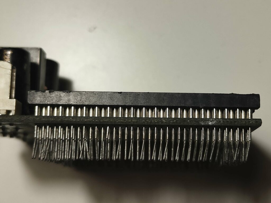
Disassembled Earlier Tubochip variant showing pin structure from edge on. Picture Credit: Carlos S.M.
The lower sockets pins have a thicker hollow tube top and a thinner lower part that fits into the motherboard socket. The pins of the top socket are also this thin at the bottom, but they are inside the socket and stuck in the lower sockets pins. The thicker part we see above the PCB is already part of the upper sockets hollow section and also prevents it going too deep into the PCB.
The parts hunt begins
Before even attempting to design a new PCB for this the first thing I had to do was figure out if all the parts I needed were actually still available. After all it wouldn’t help if I spent many hours designing this and then couldn’t actually manufacture it and assemble it.
Within a few hours of ebay hunting however I had found everything I needed. That included:
A set of interstitial PGA-321 socket made by “Max-Mill” and a set of AMP 19x19 cold formed LIF sockets was soon acquired.
The set of items I ordered. Unfortunately sources are somewhat limited.
Practically only one seller holding stock of exactly what is needed at reasonable prices.
Well the sockets arrived and they looked just about perfect for my use case. Notably the pins are not Gold Plated, but rather tinned.
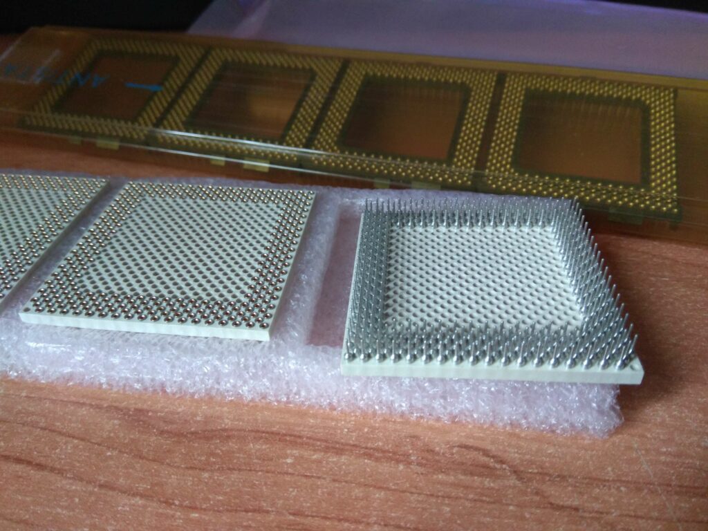
Max-Mill PGA-321 LIF interstitial sockets and in the background the 19x19 cold formed CPU LIF sockets.
Now I mentioned earlier that it was important that the sockets are soldered in the Kingston Turbochip design. The reason I say this is because I went about testing how the CPU socket stack affected the stability/reliability and otherwise characteristics of a Pentium processor.
That is how this abomination came to be:
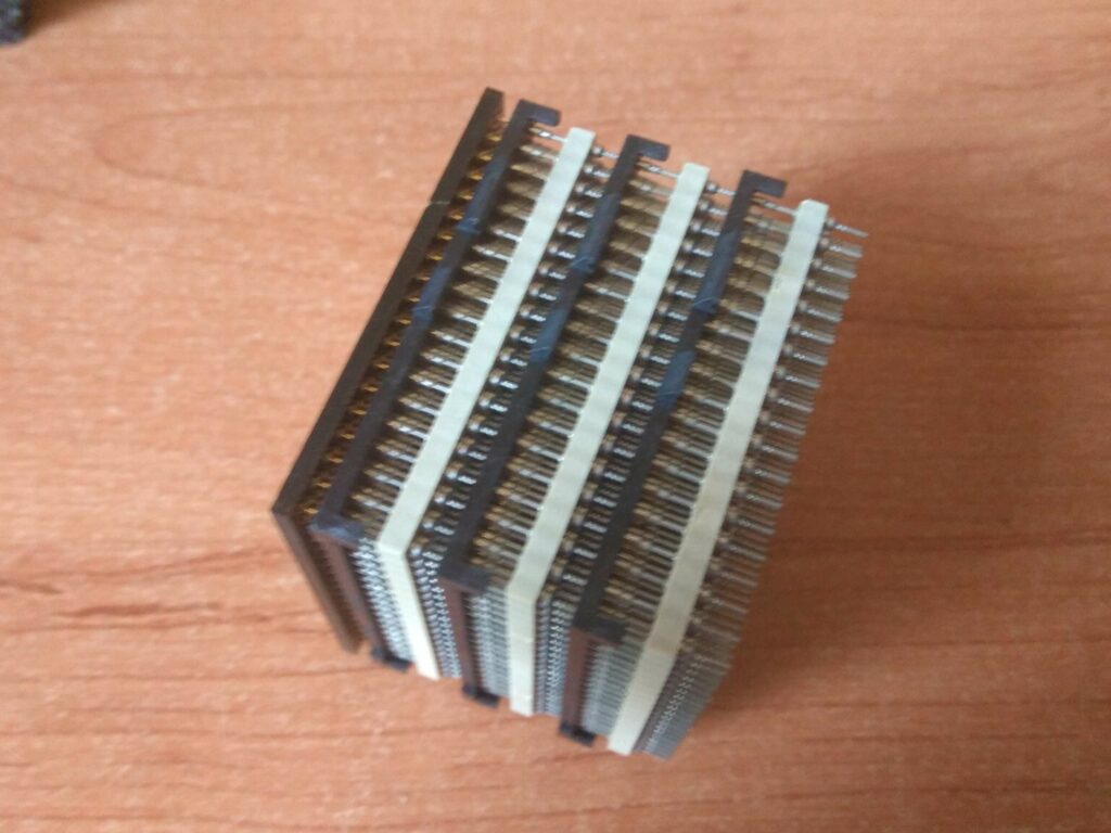
6 sockets stacked into each other with a Pentium on top. Each is made of 1 interstitial + a CPU socket.
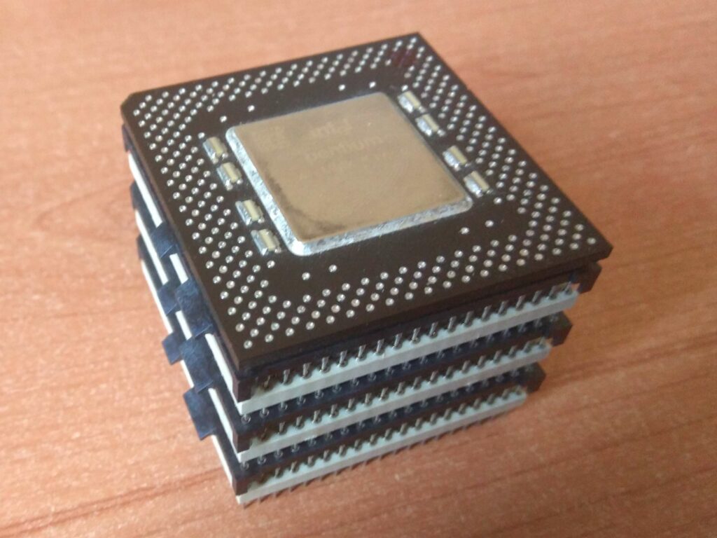
Leaning tower of Pentium... anyone?
As it turned out the only really stable configuration was one interstitial stacked into one socket, with the pins very tightly wedged into each other.
Combinations of 2 doubled sockets or more led to inconsistent results since even with two sockets I was effectively bridging through 4 interfaces.
- The CPU Pins itself
- The upper socket
- The interstitial socket
- the motherboard socket.
With 6 sockets as pictured it was a rather glitchy mess.
The PCB
So I got started then, threw together a Socket 7 Symbol file with all the pins documented, created a clean Socket 7 footprint (I know one already existed, but upon review I found it to be faulty, the holes were too large and the margins between hole+plating was too small for routing any tracks.
Further there was a large amount of User Drawings in the file underneath the pin holes, which hints that this file was actually auto-generated with some tool.
So here it is then:
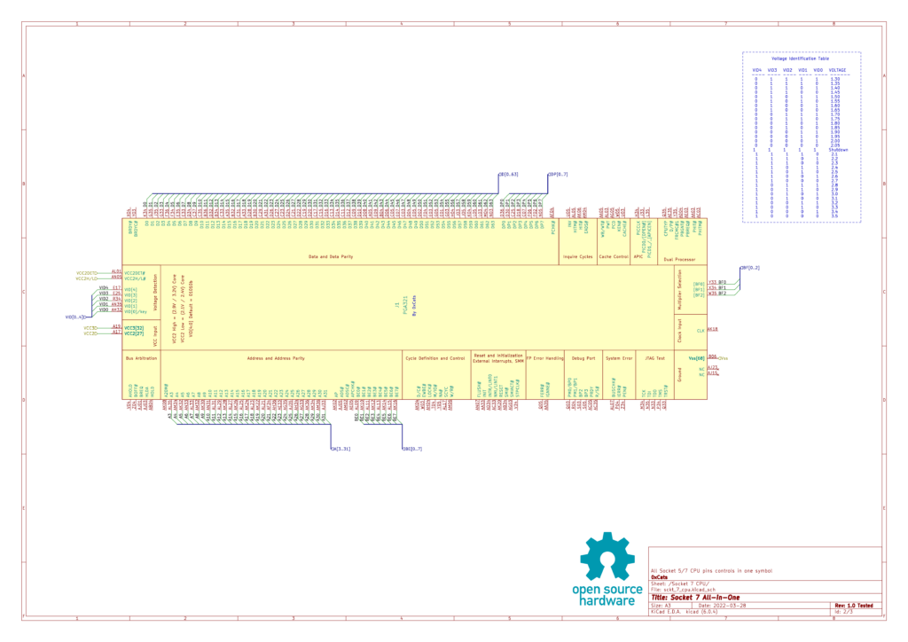
Socket 5/7 PGA-321 All CPU’s in one Symbol Diagram.
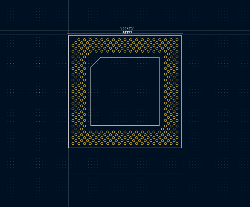
Socket 5/7 Footprint
The files and more associated with this can be found at my GitHub repository:
https://github.com/rigred/kicad-retro/tree/main/processors/socket%207
Finding a Voltage Regulator
Further to this we needed an applicable switching regulator controller. Preferably one that supports 5-bit VID input for easy voltage control and AMD K6 PowerNow support.
Several options come into question:
- Analog Devices
- ADP3154
- Cherry (Now OnSemi) (Small BOM, nice regulation, almost not supply)
- CS5161/66
- CS5150/5151
- Elantec (made by Intersil)
- EL7571/7556
- ST L6911C
- National Semiconductor
- LM2636
- LM2635
- Raytheon/Fairchild
- RC5051/53/54/57 (Small BOM, good regulation, unstable supply)
- RC5041/42
- LinFinity
- LX1660/61
- LX1662/63
- LX1664/65 (Very low cost part)
- Linear
- LTC1552/3 (Still in production, small BOM)
- LT1430/35
- LT1753 (Still in production, small BOM)
- Harris (Now Intersil)
- HIP6004/5/14 (Already have some, Large BOM)
- HIP6002/3
- HIP6019 (4 different output voltages, suitable for motherboards)
- Maxim
- MAX1624
- MAX1636 (Very impressive, shooting for the stars) But OH GOD THE PRICE!
- MAX1710 (Only up to 2.1V for Mobile K6-2+)
- Semtech (Large BOM, low efficiency)
- SC1151/52
- SC1172/73
- SC1182/83
- SC1186
- Texas Instruments TPS5210 (Could be nice but availability is poor)
- Micro Linear (Can’t find supply)
- ML4900
- ML4902
- Unisem (Can’t find supply)
- US3004 (very poor efficiency)
- Unitrode (Can’t find supply)
- UCC3882 (1.8V min, poor efficiency)
Of all of them with the exception of a very select few however come with a major caveat.
They require a ridiculous amount of input and output capacitance to get a stable output. They also require two fairly large inductors to handle the current swings inherent to the type of single phase regulation used.
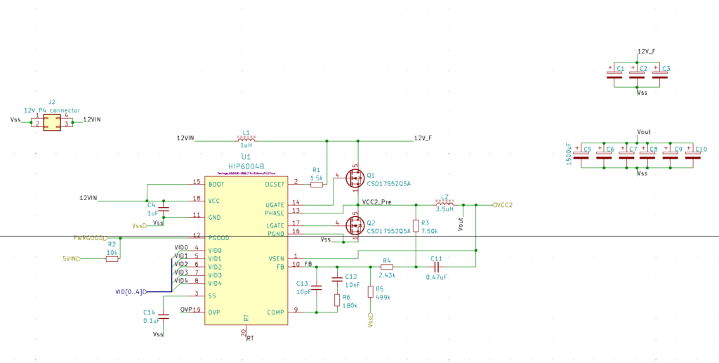
One possible HIP6004BCB based circuit that can deliver absolute excessive amount of current from the MOSFET’s.
Note the forest of Input and Output capacitance.
In the image below you can see a prototype PCB where I tested the space required to assemble the minimum viable PCB using the HIP6004BCB.
Why the HIP6004BCB? Because I already have at least 10 of them from a prior board repair, so logically it would make sense to attempt to use them rather than buy more new chips.
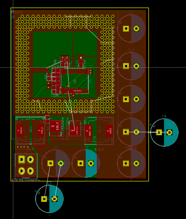
SoCat-57 Prototype 1 (HIP6004BCB Variant) - March 2022
Now technically this amount of capacitors may well be overkill for even the hottest most power hungry Cyrix M2 chip in full load swing. The design is actually based on a worst case scenario design for a Pentium 3. Even in 3D this looks fairly ridiculous. But it would at least work for my particular use case, as a minimum viable Socket-5-to-7 adapter for testing. And as part of that testing I could remove/change as many capacitors/resistors/inductors as needed to see what yields a minimum viable stable working result for Socket 7 CPU’s.
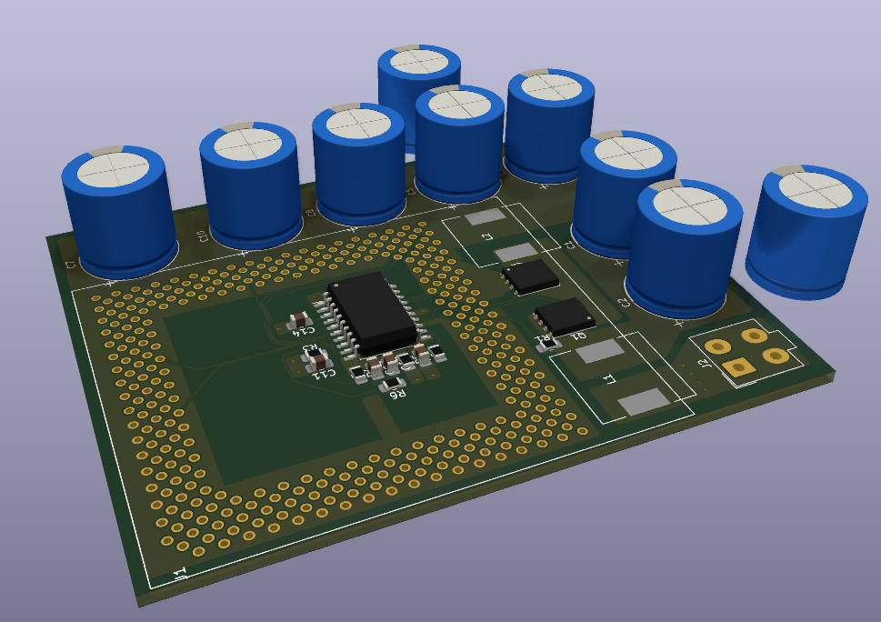
Ridiculous prototype HIP6004BCB based Socket-5-to-7 interposer design.
Now lets take a look at this LuckTech SYE-5700 motherboard. It is absolutely crowded. And my Dual Socket 5 board is not much better. The aim is for our interposer to fit that, so a wide variety of people can use it with a minimum of effort.
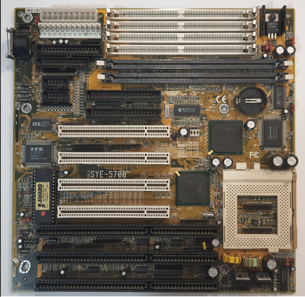
LuckyTech SYE-5700 motherboard with a horrendous socket area clearance. Who even designed this?
I have CPU coolers that have problems fitting on here, oh nevermind.
Clearly there are complex topics to be solved still before we can even get to the physical design or “Style” of the PCB, I have figuratively been spinning in circles finding a set of parts that work together optimally, result in a viable stable voltage output under various expected load conditions, while also remaining cool enough yet somehow still fitting the dimensional constraints given by the Socket 7 ZIF shape and average board layouts (Capacitors Intruding/Close to the Socket).
Now you may ask, but Cat, why don’t you put the regulators on a separate PCB and connect it via a cable? Well the reason is simple, cables are variable, they affect the circuit impedance, capacitance and lead to resistivity losses. For a minimum viable Socket 7 interposer VRM the design needs to be capable of handling at least ~12A in the 1.8V to 3.5V range. Now that may not sound like much until you realize that 12A through most cables even at such a low voltages leads to some resistivity voltage drop around 2-5% worst case if someone is using aluminium cables. Resistivity heating remains somewhat insignificant with most losses occurring in the feedback loop depending on the cable length and characteristics. Furthermore moving the supply far away from the load via a cable can create other problems such as placement, how far away is good for placing it nicely within the case, vs too far to cause output problems.
Modular Prototype V0.2
However, there is an alternative.
The IDC 2x17 connector. Or more colloquially known as the 34 pin floppy connector.
We have run out of space in the horizontal plane on our Interposer, however as architects and civil engineers understand full well, when you can’t expand outwards, you expand upwards.
Thus was born the modular VRM. This may look much like the Pentium Voltage Regulator module, but unlike the Pentium module we are using 34 instead of 30 pins and more of them can carry electrical current, additionally a few are reserved for control signals.
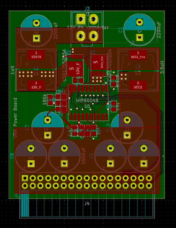
SoCat-57 VRM Module Prototype v0.2
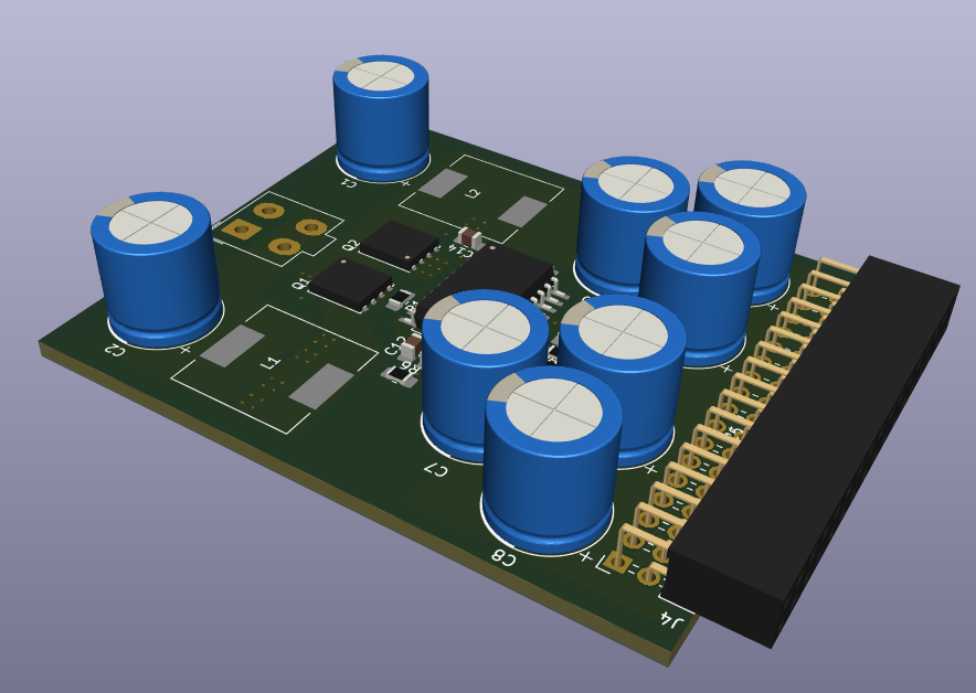
3D Rendering of the SoCat-57 Interposer Prototype V0.2
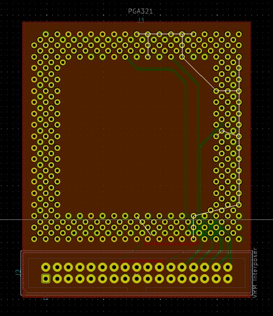
SoCat-57 Interposer Prototype V0.2
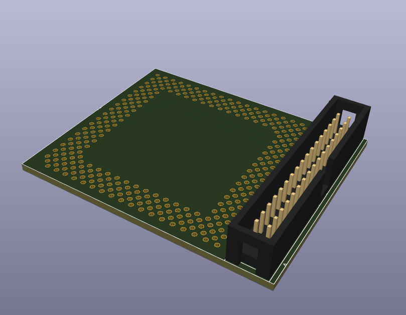
3D Rendering of the SoCat-57 Interposer Prototype V0.2
Now even this prototype will change a bit for the next variant as I will seek to move some of the components around and find the most optimal design.
This is what Engineering is all about, solving problems within given constraints.
As part of that I am also testing a few options to create a multi variant PCB that can accept other regulators on the same board with slightly shifted footprints arrangements.
Anyways that is where I will leave it for now.