Decoding the Mystery: Uncovering Missing Jumpers on a SiI0649 IDE Card Clone
Introduction
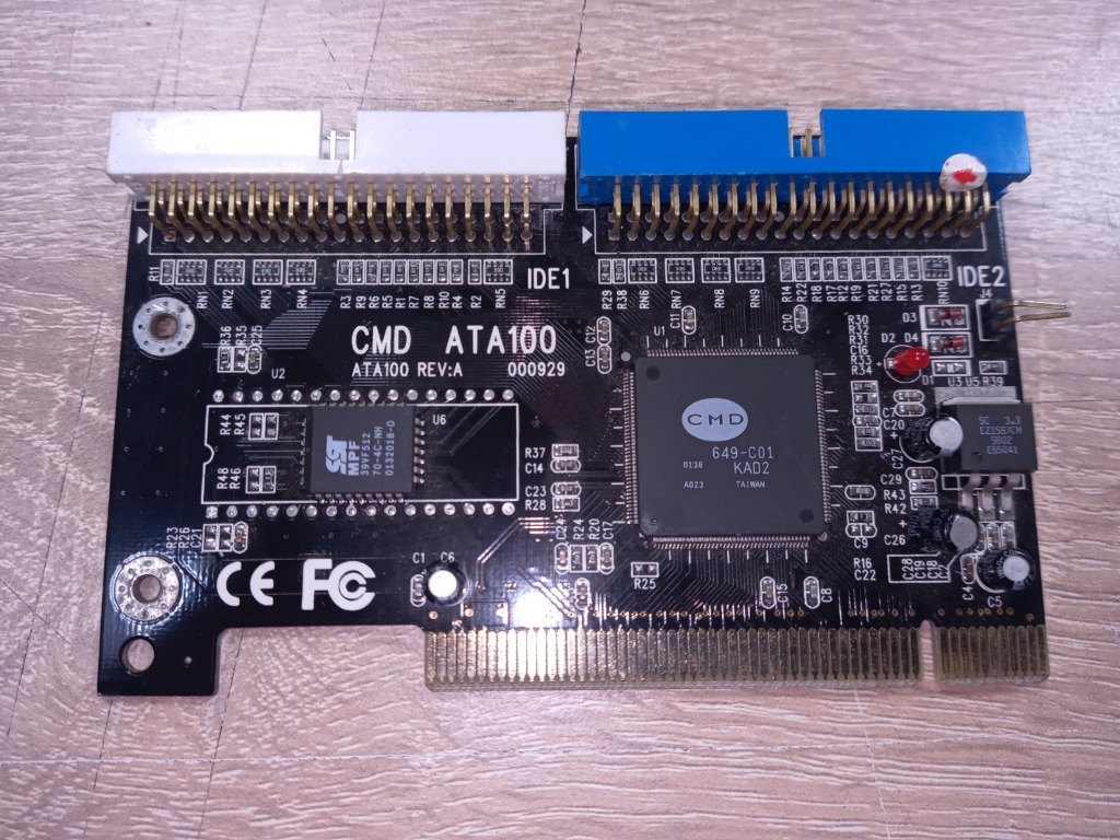
The CMD-649 Or Silicon Image 649 (Si later acquired CMD) or in my case SiI0649CL160 is a PCI IDE controller chip that has been around for quite some time. Lots of variations of these exist, and can often be cheaply bought new from AliExpress or Ebay. It’s an easy way to add ATA-6 100MB/s IDE support to boards that may be limited to 33MB/s ATA. Drivers are available for DOS, Windows 95/98, Windows Millennium, Windows NT 4.0, and Windows 2000, XP etc. The chip is also compatible with default Microsoft IDE drivers.
This vintage device usually has a few jumpers on its board, most of which are soldered and can be a bit of a challenge to figure out due to the lack of documentation. In this post, I will delve into how I reverse-engineered the missing jumpers and traced them back to the controller chip. I’ll also provide a link to the datasheet of the chip, an image of my findings, and additional information to help contextualize the jumper settings and understand where each feature may come in handy.
Variants
This card exists in quite a few forms, both with the original CMD 649 chip and the relabeled Silicon Image branded variation.
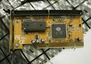
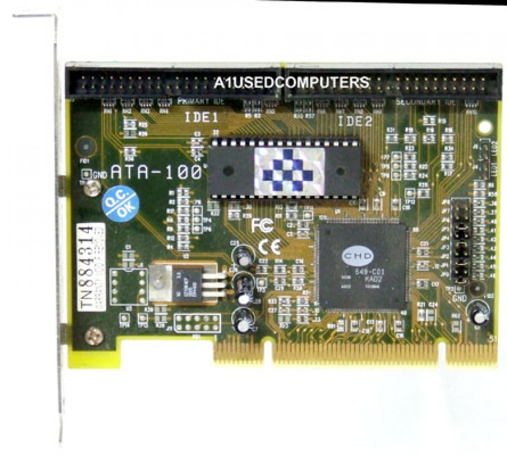
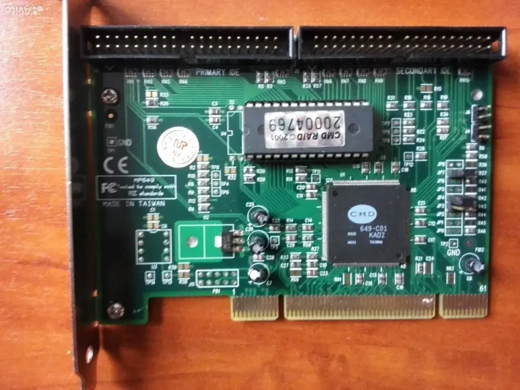
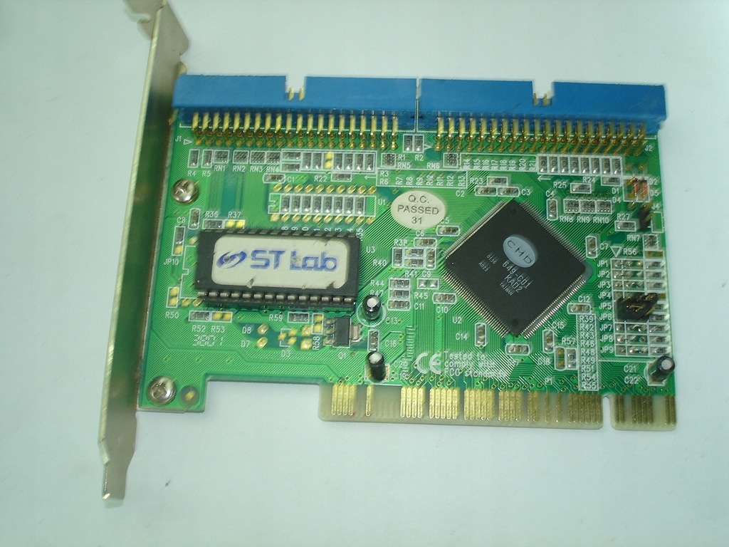
Gallery of CMD-649 variants.
Unlocking Compatibility with Older Motherboards
By default, the CMD-649 operates as a PCI RAID storage device with a PCI class code of 0104 instead of a PCI IDE device with a class code of 0101.
If you are seeking to add an IDE card to an old 486 or Socket 5 board that lacks onboard IDE, or you just want a faster IDE interface, This can cause compatibility issues with older motherboards that may not recognize the card as an IDE device and thus prevent drive detection or direct booting.
Helpfully It also features it’s own Option ROM that allows attaching up to 128GB size IDE drives onto motherboards with a BIOS that may be limited to only 8GB.
Though due to these cards often running in RAID mode by default this presented some issues and prevents direct booting as well as necessitating installing drivers as part of the Operating system install.
The Datasheet
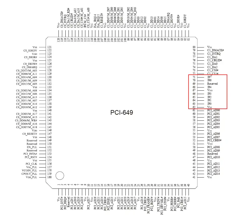
To start with, I managed to find the datasheet for the CMD-649 chip on theretroweb.com. This was a critical resource for understanding the chip’s various functions and pinout. You can find the datasheet here at theretroweb chip database.
CMD 649-C01 (UDMA 5 IDE controller)
Get expansion chip info, images and drivers for CMD 649-C01 (UDMA 5 IDE controller)!
There I could get a pin map, with specifically the pins we are interested in boxed in red:
Reverse Engineering the Jumpers
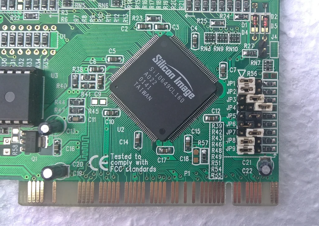
Using the datasheet as a reference, I began tracing the jumper traces to the chip. This allowed me to determine the purpose of each jumper and their corresponding pins on the CMD-649 chip. The image below shows the jumper traces and their connections to the chip. It turns out the designers of my particular card simply reversed all of the jumpers from the design and started counting at 1 instead of 0.
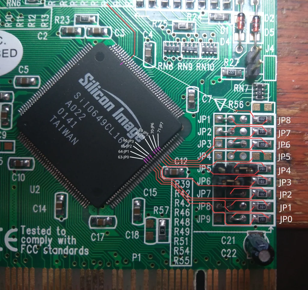
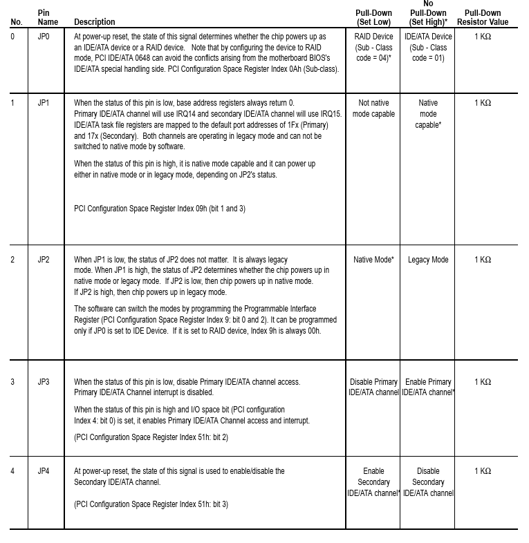
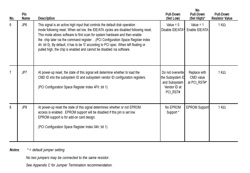
Understanding the Jumper Settings
After completing the trace, I compiled the jumper settings in a table by cross referencing it to the datasheet Jumper pins.
This table lists the jumper number, jumper setting, function, default jumper setting, and CMD-649 datasheet jumper. The jumper settings provide various functionalities that can be helpful in different scenarios. Here, I have outlined some of these features and their possible applications.
| Function | Jumper | Setting | Default | Pin |
|---|---|---|---|---|
| Enable RAID BIOS PCI Scan for attached devices. | JP1 | 1-2 | 1-2 | JP8 |
| Disable RAID BIOS PCI Scan for attached devices. | JP1 | 2-3 | ||
| Replace SID/SVID with CMD values at PCI_RESET# | JP2 | 1-2 | 1-2 | JP7 |
| Do not overwrite System ID/Subsystem Vendor ID at PCI_RESET# | JP2 | 2-3 | ||
| Chip IO space access is enabled, and cannot be disabled | JP3 | 1-2 | 2-3 | JP6 |
| Chip IO space access is disabled, but can be enabled | JP3 | 2-3 | ||
| This jumper is not valid anymore, It changed to TEST1 pin. | JP4 | N/A | Open | JP5 |
| Disable secondary ATA/100 channel | JP5 | 1-2 | 2-3 | JP4 |
| Enable secondary ATA/100 channel (Default) | JP5 | 2-3 | ||
| Enable primary ATA/100 channel (Default) | JP6 | 1-2 | 1-2 | JP3 |
| Disable primary ATA/100 channel | JP6 | 2-3 | ||
| IDE channels 0 and 1: Power up mode is Legacy | JP7 | 1-2 | 2-3 | JP2 |
| IDE channels 0 and 1: Power up mode is Native (Default) | JP7 | 2-3 | ||
| IDE channels 0 and 1: Mode is programmable (Default) | JP8 | 1-2 | 1-2 | JP1 |
| IDE channels 0 and 1: Mode is fixed | JP8 | 2-3 | ||
| IDE Device with 0101h at PCI config | JP9 | 1-2 | 2-3 | JP0 |
| Non IDE Device with 0104h at PCI config (Default) | JP9 | 2-3 |
If you are curious here are the specific descriptions from the datasheet for each of the jumper bootstrap pins. Remember to cross reference these to the datasheet pin in the last column of my above table.
Modified Card
A little bit of soldering later and we’ve got a total of 8 jumpers. Yay!
Here you can see that I have reconfigured the card to the IDE operating mode (JP9) and left the Option ROM enabled. This is useful as I discovered that even in IDE mode that Option ROM can scan for IDE drives and detect up to 128GB size disks on otherwise limited boards. If you’re using this make sure to disable the onboard IDE controller. You can use both but the chance for resource conflicts is likely.
Conclusion
Reverse engineering the CMD-649 PCI IDE controller card jumpers was an intriguing little project that allowed me to better understand the device’s functions and configurations.
Hopefully this information can also be helpful for those who are working with these.