Deconstructing the Kunpeng 916: A Community-Driven Deep Dive
Some of the best stories in hardware start not in a corporate lab, but in a corner of the internet where enthusiasts gather. This is one of those stories. It’s about a piece of silicon that’s both pivotal and poorly documented: the HiSilicon 1616, also known as the Kunpeng 916. And it begins, as these things often do, with a simple message on Discord.
The Discovery
The scene was the Xeon Phi Discord, a place for folks who appreciate esoteric hardware. A user named Resbi dropped a message that immediately caught my attention:
Resbi — 9 July at 16:51
I got ssh to a Hi1616 2x32 cores TaiShan 2280 server
Suddenly, a special beast was on the network. The Kunpeng 916 (Hi1616) is a fascinating chip. Released around 2017, it was one of Huawei’s first serious forays into multi-socket ARM server CPUs, a shot across the bow of the x86-dominated data center. But unlike its more modern successors, its inner workings are largely a black box.
The basic specs of the Kunpeng 916 (formerly Hi1616) are as follows:
- 32x ARM Cortex-A72 at up to 2.4 GHz
- 48 KB L1-I, 32 KB L1-D, 1 MB L2/4 cores and 32 MB CCN L3
- Manufactured on TSMC 16 nm
- 4x DDR4-2400 channels
- 2-way Symmetric multiprocessing (SMP), Each socket has 2x ports with 96 Gbit/s per port (total of 192 Gbit/s per each socket interconnects)
- 46 PCIe 3.0 and 8x 10 Gigabit Ethernet
- 85 W TP
Armed with access and the Chips and Cheese microbenchmarking toolkit, Resbi started pulling data. And that’s when things got weird.
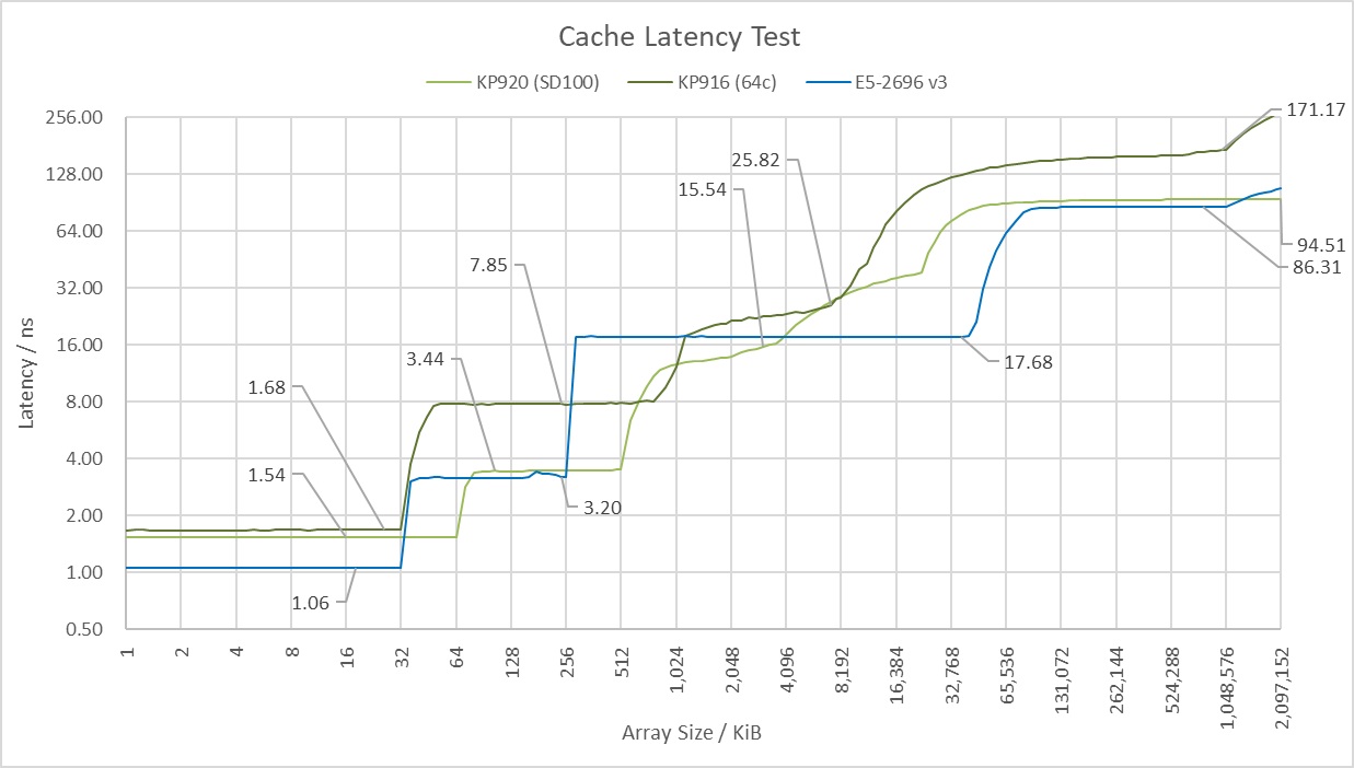
The initial results from the cache latency test were baffling. The public specs for the Kunpeng 916, primarily from sources like WikiChip, claim it has a 32 MB L3 cache. But the data showed something else entirely. The graph paints a clear picture of the memory hierarchy. hi1616
- L1 Cache: Access is incredibly fast, around ~1.6ns, for the first 32 KB, which corresponds perfectly to the L1 data cache of the ARM Cortex-A72 core.
- L2 Cache: Latency then steps up to around ~7.85ns for the L2 cache region, which extends out towards 1 MB. This aligns with the 1 MB L2 cache shared per quad-core cluster.
- L3 Cache & The Cliff: After an L2 miss, we enter the L3 domain. Here, latency settles at a respectable ~25 ns, but only up to an 8 MB data size. Beyond that point, performance falls off a cliff, heading straight for the slow lane of main memory at over 120 ns around 32MB. At 16MB we are seeing about ~70-80ns.
This “8 MB cliff” was a mystery. It proves the 32 MB L3 isn’t uniform, but it raised more questions than it answered.
“X-Raying” the Chip
A core-to-core latency test is the perfect tool for this. It measures how long it takes for every core to communicate with every other core, producing a heatmap that reveals the physical topology of the system.
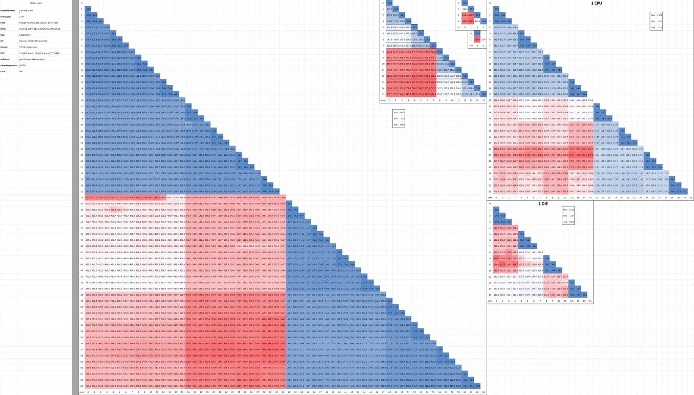
The resulting 64x64 matrix was a beautiful, symmetrical blueprint of the server’s architecture. Reading it layer by layer, the structure became clear:
-
Two Sockets: The map was split into four big 32x32 quadrants. Communication within the first 32 cores and within the second 32 cores was fast (blue). Communication between the two groups was slow (red). Classic dual-socket system. This confirmed the “2x32 cores” in Resbi’s initial message.
-
Two Dies Per Socket: Zooming into a single 32-core socket, we saw another split. Cores 0-15 could talk to each other faster than they could talk to cores 16-31. This was the smoking gun for a Multi-Chip Module (MCM) design. Each 32-core Kunpeng 916 CPU wasn’t one monolithic piece of silicon, but two 16-core dies living in the same package. As Resbi confirmed: “YES… 1 die has 16 cores”. HiSilicon refers to these two compute dies as the Super CPU cluster (SCCL).
-
Two Clusters Per Die: Digging even deeper into a single 16-core die, we saw yet another boundary. Cores 0-7 communicated faster with each other than with cores 8-15. This meant each 16-core die was composed of two 8-core clusters.
The physical layout was solved. Each 32-core CPU consists of two dies, and each die contains two 8-core clusters. That gives us a total of four 8-core clusters per CPU.
This discovery was the key.
The “Aha!” Moment
I started connecting the dots. The physical map showed four distinct 8-core domains. The latency test showed a fast 8 MB cache domain.
32 MB total L3 cache / 4 clusters = 8 MB per cluster
The Kunpeng 916 does have 32 MB of L3 cache, but it’s not a single, uniform pool of memory. It’s a Non-Uniform Cache Access (NUCA) system. The “32x1MB” L3 cache spec from WikiChip, initially confusing, now makes perfect sense. It suggests a highly granular NUCA design.
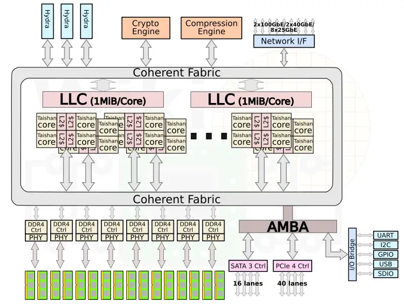
After some digging, the official terminology started to make sense. A one-line comment on WikiChip’s HiSilicon 16xx family page mentions a “CCN L3.” The Cache Coherent Network (CCN) is the on-chip fabric that connects these clusters and their L3 slices. hi16xx
Here’s how it works:
The Cache Coherent Network (CCN) is the key. It likely manages the L3 as 32 individual 1 MB slices. Within each 8-core cluster, a local directory controller manages the cluster’s 8 MB portion of the L3. This creates multiple NUCA tiers:
- When a core needs data beyond L1 or L2 it queries its local cluster’s directory. It’s plausible each core has a “home” 1MB L3 slice that is physically closest to it, offering the absolute lowest L3 latency.
- If the data resides in one of the other 7 L3 slices within the same 8-core cluster, the CCN routes the request internally. This trip across the cluster’s local network averages out to the ~25 ns latency we see in the graph for the 8 MB region.
- If the data is not in the local 8 MB cluster cache, the request is broadcast over the CCN to the other clusters on the same die. A hit in a remote L3 slice requires this extra hop, causing the latency to jump. This is the “8 MB cliff” we see at around ~70-80ns.
- If the data isn’t on the chip at all, the request goes out over the Huawei Cache Coherency System (HCCS), the interconnect for die-to-die and socket-to-socket traffic, incurring the highest latency penalty as it fetches from another CPU or main memory.
The mystery was solved. The weird performance wasn’t a bug or a case of a “missing” cache; it was a feature of a complex, hierarchical design.
Update: Confirmed Architectural Details
Further system-level analysis using numactl and lscpu provided a ground-truth confirmation of the Kunpeng 916’s architecture, validating the initial microbenchmark results and revealing a deeper level of complexity.
System Topology and NUMA Layout
- Four NUMA Nodes: The dual-socket 64-core system presents to the operating system as four distinct NUMA nodes. Each 16-core die within a CPU package constitutes a single NUMA node.
- Socket 0: Contains NUMA Node 0 (Cores 0-15) and NUMA Node 1 (Cores 16-31).
- Socket 1: Contains NUMA Node 2 (Cores 32-47) and NUMA Node 3 (Cores 48-63).
available: 4 nodes (0-3)
node 0 cpus: 0 1 2 3 4 5 6 7 8 9 10 11 12 13 14 15
node 1 cpus: 16 17 18 19 20 21 22 23 24 25 26 27 28 29 30 31
node 2 cpus: 32 33 34 35 36 37 38 39 40 41 42 43 44 45 46 47
node 3 cpus: 48 49 50 51 52 53 54 55 56 57 58 59 60 61 62 63
- Quantified Latency: The relative latency costs for memory access across the interconnect are now quantified:
- Intra-Die (Local): Baseline latency cost of
10. - Inter-Die (Same Socket): Latency cost of
15. - Inter-Socket (Remote CPU): Latency cost of
20.
- Intra-Die (Local): Baseline latency cost of
node distances:
node   0   1   2   3
  0:  10  15  20  20
  1:  15  10  20  20
  2:  20  20  10  15
  3:  20  20  15  10
Integrated I/O, Not a Chiplet
The final mystery was whether the Kunpeng 916 used a separate I/O die like its successor. The PCIe Device NUMA Affinity section of the log gave a clear answer: No.
7. PCIe Device NUMA Affinity
==============================================================================
  0002:e8:00.0  node 0  bridge: Huawei Technologies Co., Ltd. Device 1610
  0004:49:00.0  node 1  Attached SCSI controller: Broadcom / LSI SAS3008
  000d:31:00.0  node 3  compatible controller: Advanced Micro Devices, Inc. [AMD/ATI] Ellesmere
The output shows PCIe devices, including an AMD GPU and a SAS controller, are attached to different NUMA nodes. This confirms that I/O controllers are integrated directly onto the compute dies, making the Kunpeng 916 a more monolithic System-on-a-Chip (SoC) design rather than a chiplet-based one.
What This Architecture Is Good For
This deep, hierarchical design is a deliberate trade-off. It sacrifices uniform low latency for massive parallelism and throughput. This makes the Kunpeng 916 specialized.
-
Strengths: This CPU is built for workloads that can be neatly partitioned and spread across its many cores. Think scientific computing, large-scale data processing, and other throughput-oriented tasks. If you can design your problem so that each 8-core cluster is mostly working on data within its local 8 MB L3 slice, you can unleash the full power of the chip.
-
Weaknesses: It will struggle with tasks that have poor data locality. A single-threaded application with a large, randomly accessed working set (>8 MB) will constantly pay the NUCA latency tax as it fetches data from remote cache slices.
How to Program for It
For anyone writing software for this hardware, the takeaway is simple: you must be NUMA-aware. The detailed topology underscores this critical need. For optimal performance, processes should be pinned not just to a specific CPU socket, but to the specific 16-core NUMA node (die) that provides the lowest latency access to the required resources.
-
Pin Your Processes: Use tools like
tasksetornumactlto lock your applications to the cores within a specific physical domain (e.g., cores 0-7 for an 8-core cluster, or 0-15 for a full die). -
Place Your Memory and Peripheraps: Thread pinning is useless if the data or devices live on another die. For example, since the log shows the AMD GPU is on NUMA node 3, a GPGPU application should have its threads and memory explicitly bound to that node to avoid the 1.5x-2.0x latency penalty of cross-die communication:
numactl --physcpubind=48-63 --membind=3 ./my_gpu_application -
Design for Locality: The best approach is to design algorithms that respect the hardware. Keep the “hot” working set for latency-sensitive tasks within the 8 MB local L3 slice.
Looking Forward to Look Back: What the Kunpeng 920 Tells Us
Often, the best way to understand a piece of technology is to look at what came next. The Kunpeng 920, the successor to our mysterious 916, is a perfect example. While details on the 916 are scarce, information on the 920 is more available, and it acts as our Rosetta Stone, confirming many of the theories we developed here.
Looking at the Kunpeng 920’s architecture, we can see a clear evolutionary path from the 916. This isn’t a revolution; it’s a refinement of a consistent design philosophy.
-
The Sliced Cache Philosophy is Confirmed: The Kunpeng 920 features a large L3 cache that is explicitly described as “1 MiB per core.” This validates our discovery that the 916’s L3 is a granular, distributed NUCA design.
-
The Interconnect’s Family Tree: The Kunpeng 920 uses a high-speed, proprietary interconnect called the Huawei Cache Coherency System (HCCS) for multi-socket communication, implemented with ports codenamed “Hydra”. The Kunpeng 916 was the first chip in the family to support 2-way SMP, so it stands to reason that it contains the first generation of this HCCS interconnect. The distinct latency tiers we measured in the core-to-core heatmap are the performance fingerprint of this “Proto-HCCS” fabric.
-
An Evolving Chiplet Strategy: Both processors are Multi-Chip Modules (MCMs), but they show a clear evolution in strategy. The 916 uses a simpler design: two identical 16-core compute dies packaged together. The 920 takes this a step further into a more advanced chiplet architecture, using multiple dedicated compute dies (called SCCL) and a separate, dedicated I/O die (SICL). This shows a consistent belief in scaling performance by adding dies, with the design becoming more sophisticated and disaggregated over time.
-
A Shift in Mid-Level Cache Design: One of the most significant architectural changes between the two generations is the L2 cache. The 916 uses a 1 MB L2 cache shared between four Cortex-A72 cores, a common configuration for licensed ARM cores of that era. The Kunpeng 920, with its custom TaiShan v110 cores, moves to a large, private 512 KB L2 cache for every single core. This is a major shift, likely aimed at boosting single-thread performance and reducing cache contention within a core cluster, a trend common across modern high-performance server CPUs.
-
The Integrated SoC Philosophy: The 920 is a full System-on-a-Chip, integrating I/O controllers and even hardware accelerators for crypto and compression directly onto the package (specifically, the I/O die). The 916 also integrated significant I/O like PCIe and 10GE networking, showing that from the beginning, Huawei’s strategy was to create a complete platform solution on-chip, reducing the need for external support chipsets.
The Final Word
The deconstruction of the Kunpeng 916 is a good example of community-driven reverse engineering. What started as a confusing benchmark result on a Discord server evolved into a detailed architectural model that explains the “why” behind the chip’s performance.
The ultimate validation, however, comes from looking at the architectural roadmap that followed. The Kunpeng 920, with its explicit use of a sliced 1MB-per-core L3 cache, its advanced multi-chiplet design, and its proprietary HCCS interconnect, confirms that our findings on the 916 weren’t just theories—they were an accurate glimpse into the foundational principles of Huawei’s server architecture. The “weirdness” we observed was, in fact, the first draft of a sophisticated, hierarchical design philosophy built for a high-core-count, throughput-oriented world. Huawei Expands Kunpeng Server CPUs, Plans SMT, SVE For Next Gen
Thanks to the curiosity of users like Resbi and the collaborative power of the hardware community, we now know that the Kunpeng 916 is more than just an old server chip. It’s a critical link in an evolutionary chain, a processor that offers a clear view into the design trade-offs necessary to build modern server CPUs. And for those who understand its nature, it remains a powerful tool for parallel computing.