SIMMBA-16.P a 30 pin SIMM
SIMMBA-16.P is an open-source, 30-pin SIMM memory module with a maximum capacity of 16MB. It is designed to be low-cost, simple, and flexible in terms of RAM chip and socket selection. This project is perfect for vintage computer enthusiasts who want to maximize the memory capacity of their 486 motherboards that feature a mix of 2x72-pin and 4x30-pin SIMM sockets. With the rising prices of 30-pin SIMM memory modules, SIMMBA-16.P offers an affordable alternative. Check out our GitHub repo for more information.
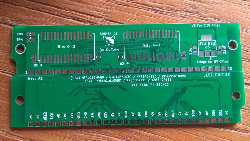
The first A1 revision PCB, this was before the SIPP hole connector edge was added.
Key Features
- 16MB maximum capacity
- 30-pin SIMM/SIPP compatibility
- Flexible RAM chip and socket selection
- FPM/EDO operation selection
- Open-source design
Why?
Because I have a 486 motherboard that I’m quite fond of that featured a mix of 2x72pin and 4x30pin SIMM sockets. I wanted to use both at maximum capacity. Also 30 pin SIMM memory prices are not great.
Supported RAM chips
3.3V chips may be relatively easily found from cheaply available 256MB EDO DIMM’s. These are by far the preferred choice in comparison to the now rarer 5V chips. I have tested and validated some of the below chips and found them to be 5V IO tolerant in use despite manufacturer data sheets not directly ascribing such. Of these the Micron chips are by far the most common and robust. All others have been data sheet checked to be electrically compatible.
(3.3V)
- MT4LC16M4H9 (Preferred, Tested & Validated)
- GM71V65403C (Tested)
- K4F640412C (Validated)
- KM44V16104BK (Validated)
(5V)
- KM44C16100BK
- K4E660411C
- K4F640411B
RAM Salvaging
If you plan on salvaging compatible chips from DRAM modules, follow these guidelines to ensure a smooth process:
- Test the source RAM boards before salvaging to ensure the quality of the chips.
- Use a preheater and hot air station or temperature-controlled reflow oven to remove the chips without overheating them.
- Expect some challenges if you haven’t done this before, but don’t give up.
- Keep in mind that I cannot be held responsible for any issues that may arise during this process.
Voltage selection
- When 3.3V chips are used it is required to install a suitable 3.3V LDO regulator such as the common AMS1117-3.3 as well as the 10uF Capacitor
- When 5V chips are used you must bridge the indicated pads with a 0-Ohm resistor or suitable piece of metal and install the 22uF Capacitor
- DO NOT install the 3.3V Regulator when using 5V chips and bridging the indicated pads.
EDO / FPM selection
For the most part only the FPM bridge should be populated. In this mode the CAS signal is tied to the Output Enable signal pin of the chips. On EDO DRAM chips this forces the output buffers to become invalid and cleared as soon as the CAS is toggled and allows EDO chips to behave like FPM chips. In rare cases you may want to configure this module as EDO mode, such as in use with 72pin to 4x30pin SIMM-Saver/SIMM-Expander boards.
SIPP mode
If you wish to use these as SIPP modules, in case say your SIMM sockets are broken, or you’ve found some very obscure motherboard that both supports SIPP memory and this size of module. Then you can simply solder a right angle 100mil/2.54mm header to the holes along the edge.


Assembly
gerber.zip
Ordering specifics:
- 1.2mm Thickness
- HASL or ENIG (any finish is fine)
Bill of Materials
Soldering
- For repeatable good results when soldering the ram chips in place it is recommended to use a stencil and soldering paste and soldering the whole board in one pass on a hot plate.
- Hand soldering is possible but great care must be taken to ensure good contact on the pads and no solder bridging. Large quantities of flux recommended.
Troubleshooting
- If you are using the 3.3V regulator design and are experiencing voltage instability it may be necessary to adjust the capacitance of the 5V input and 3.3V output filter capacitors.
- In this design, less can often be better.
- After assembly it is recommended to first power test and check your handiwork in expectation of failure. Feel for any hot parts on the DRAM
- If you are getting memory errors there is a good chance that either some pins are not making good contact or you’ve overheated one of the chips.
- Mixing and matching these modules with other modules in the same bank is NOT supported nor recommended.
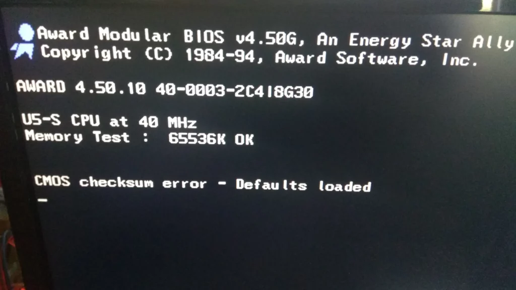
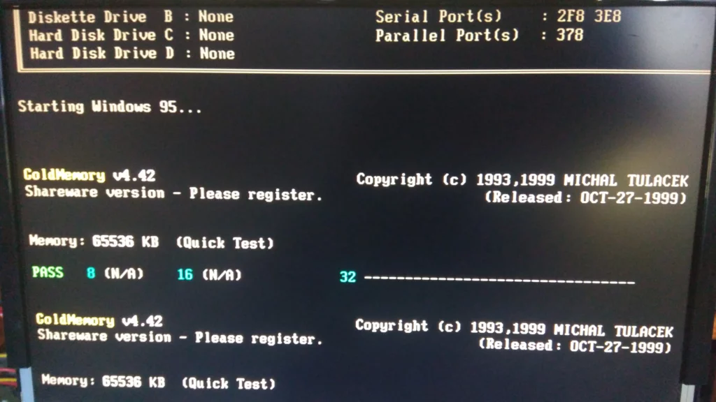
Revision A1 testing
The A1 revision SIMMBA module assembled

64MB of SIMMBA A1 revision under test

A Happy Camper with 64MB of 30 pin SIMM’s validated